- 您现在的位置:买卖IC网 > Sheet目录2006 > LTC2355IMSE-14#TRPBF (Linear Technology)IC ADC 14BIT 3.5MSPS 10-MSOP
LTC2355-12/LTC2355-14
2355fa
pin Functions
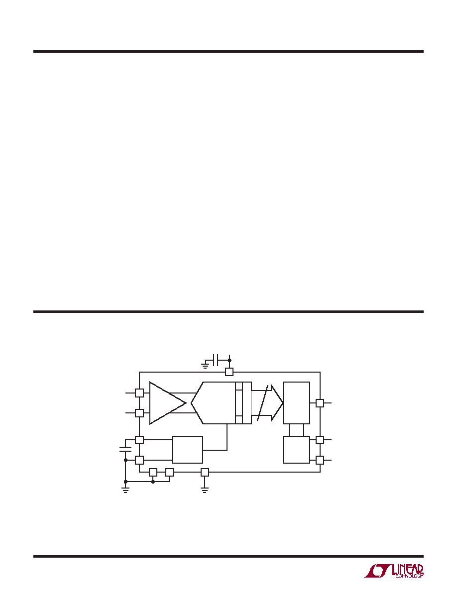
AIN+(Pin1):NoninvertingAnalogInput.AIN+operatesfully
differentially with respect to AIN– with a 0V to 2.5V dif-
ferential swing and a 0V to VDD common mode swing.
AIN– (Pin 2): Inverting Analog Input. AIN– operates fully
differentially with respect to AIN+ with a –2.5V to 0V dif-
ferential swing and a 0V to VDD common mode swing.
VREF (Pin 3): 2.5V Internal Reference. Bypass to GND
and to a solid analog ground plane with a 10F ceramic
capacitor(or10Ftantaluminparallelwith0.1Fceramic).
Can be overdriven by an external reference between 2.55V
and VDD.
GND (Pins 4, 5, 6, 11): Ground and Exposed Pad. These
ground pins and the exposed pad must be tied directly to
the solid ground plane under the part. Keep in mind that
analog signal currents and digital output signal currents
flow through these pins.
VDD (Pin 7): 3.3V Positive Supply. This single power pin
supplies 3.3V to the entire device. Bypass to GND and to
a solid analog ground plane with a 10F ceramic capacitor
(or 10F tantalum in parallel with 0.1F ceramic). Keep in
mind that internal analog currents and digital output signal
currents flow through this pin. Care should be taken to
place the 0.1F bypass capacitor as close to Pins 6 and
7 as possible.
SDO (Pin 8): Three-State Serial Data Output. Each set
of output data words represents the difference between
AIN+ and AIN– analog inputs at the start of the previous
conversion.
SCK(Pin9):ExternalClockInput.Advancestheconversion
process and sequences the output data on the rising edge.
Responds to TTL (≤3.3V) and 3.3V CMOS levels. One or
more SCK pulses wakes the ADC from sleep mode.
CONV(Pin10):ConvertStart.Holdstheanaloginputsignal
and starts the conversion on the rising edge. Responds
to TTL (≤3.3V) and 3.3V CMOS levels. Two CONV pulses
with SCK in fixed high or fixed low state start Nap mode.
Four or more CONV pulses with SCK in fixed high or fixed
low state start Sleep mode.
Block Diagram
2355 BD
–
+
1
2
7
3
4
S & H
GND
EXPOSED PAD
LTC2355-14
VREF
10F
AIN–
AIN+
14-BIT ADC
3.3V
10F
14
14-BIT
LA
TCH
8
10
9
THREE-
STATE
SERIAL
OUTPUT
PORT
2.5V
REFERENCE
TIMING
LOGIC
VDD
SDO
CONV
SCK
5
6
11
发布紧急采购,3分钟左右您将得到回复。
相关PDF资料
LTC2356IMSE-14#TRPBF
IC ADC 14BIT 3.5MSPS 10-MSOP
LTC2366HTS8#TRPBF
IC ADC 12BIT 3MSPS TSOT23-8
LTC2379HMS-18#PBF
IC ADC 18BIT SPI/SRL 16MSOP
LTC2380HMS-16#TRPBF
IC ADC 16BIT 2MSPS 16-MSOP
LTC2382HMS-16#PBF
IC ADC 16BIT 1CH 500KSPS 16-MSOP
LTC2383HMS-16#PBF
IC ADC 16BIT 1CH 1MSPS 16-MSOP
LTC2393IUK-16#TRPBF
IC ADC 16BIT SER/PAR 1M 48-QFN
LTC2410IGN#TRPBF
IC ADC 24BIT DIFF INP/REF 16SSOP
相关代理商/技术参数
LTC2356CMSE-12#PBF
功能描述:IC ADC 12BIT 3.5MSPS 10-MSOP RoHS:是 类别:集成电路 (IC) >> 数据采集 - 模数转换器 系列:- 标准包装:1,000 系列:- 位数:16 采样率(每秒):45k 数据接口:串行 转换器数目:2 功率耗散(最大):315mW 电压电源:模拟和数字 工作温度:0°C ~ 70°C 安装类型:表面贴装 封装/外壳:28-SOIC(0.295",7.50mm 宽) 供应商设备封装:28-SOIC W 包装:带卷 (TR) 输入数目和类型:2 个单端,单极
LTC2356CMSE-12#TRPBF
功能描述:IC ADC 12BIT 3.5MSPS 10-MSOP RoHS:是 类别:集成电路 (IC) >> 数据采集 - 模数转换器 系列:- 标准包装:1,000 系列:- 位数:16 采样率(每秒):45k 数据接口:串行 转换器数目:2 功率耗散(最大):315mW 电压电源:模拟和数字 工作温度:0°C ~ 70°C 安装类型:表面贴装 封装/外壳:28-SOIC(0.295",7.50mm 宽) 供应商设备封装:28-SOIC W 包装:带卷 (TR) 输入数目和类型:2 个单端,单极
LTC2356CMSE-14#PBF
功能描述:IC ADC 14BIT 3.5MSPS 10-MSOP RoHS:是 类别:集成电路 (IC) >> 数据采集 - 模数转换器 系列:- 标准包装:1,000 系列:- 位数:12 采样率(每秒):300k 数据接口:并联 转换器数目:1 功率耗散(最大):75mW 电压电源:单电源 工作温度:0°C ~ 70°C 安装类型:表面贴装 封装/外壳:24-SOIC(0.295",7.50mm 宽) 供应商设备封装:24-SOIC 包装:带卷 (TR) 输入数目和类型:1 个单端,单极;1 个单端,双极
LTC2356CMSE-14#TRPBF
功能描述:IC ADC 14BIT 3.5MSPS 10-MSOP RoHS:是 类别:集成电路 (IC) >> 数据采集 - 模数转换器 系列:- 标准包装:1,000 系列:- 位数:12 采样率(每秒):300k 数据接口:并联 转换器数目:1 功率耗散(最大):75mW 电压电源:单电源 工作温度:0°C ~ 70°C 安装类型:表面贴装 封装/外壳:24-SOIC(0.295",7.50mm 宽) 供应商设备封装:24-SOIC 包装:带卷 (TR) 输入数目和类型:1 个单端,单极;1 个单端,双极
LTC2356IMSE-12#PBF
功能描述:IC ADC 12BIT 3.5MSPS 10-MSOP RoHS:是 类别:集成电路 (IC) >> 数据采集 - 模数转换器 系列:- 标准包装:1,000 系列:- 位数:16 采样率(每秒):45k 数据接口:串行 转换器数目:2 功率耗散(最大):315mW 电压电源:模拟和数字 工作温度:0°C ~ 70°C 安装类型:表面贴装 封装/外壳:28-SOIC(0.295",7.50mm 宽) 供应商设备封装:28-SOIC W 包装:带卷 (TR) 输入数目和类型:2 个单端,单极
LTC2356IMSE-12#TRPBF
功能描述:IC ADC 12BIT 3.5MSPS 10-MSOP RoHS:是 类别:集成电路 (IC) >> 数据采集 - 模数转换器 系列:- 标准包装:1,000 系列:- 位数:16 采样率(每秒):45k 数据接口:串行 转换器数目:2 功率耗散(最大):315mW 电压电源:模拟和数字 工作温度:0°C ~ 70°C 安装类型:表面贴装 封装/外壳:28-SOIC(0.295",7.50mm 宽) 供应商设备封装:28-SOIC W 包装:带卷 (TR) 输入数目和类型:2 个单端,单极
LTC2356IMSE-14
制造商:Linear Technology 功能描述:IC ADC 14BIT 3 WIRE SPI 3.5MSPS
LTC2356IMSE-14#PBF
功能描述:IC ADC 14BIT 3.5MSPS 10-MSOP RoHS:是 类别:集成电路 (IC) >> 数据采集 - 模数转换器 系列:- 标准包装:1 系列:microPOWER™ 位数:8 采样率(每秒):1M 数据接口:串行,SPI? 转换器数目:1 功率耗散(最大):- 电压电源:模拟和数字 工作温度:-40°C ~ 125°C 安装类型:表面贴装 封装/外壳:24-VFQFN 裸露焊盘 供应商设备封装:24-VQFN 裸露焊盘(4x4) 包装:Digi-Reel® 输入数目和类型:8 个单端,单极 产品目录页面:892 (CN2011-ZH PDF) 其它名称:296-25851-6